
Isolated Power Supplies
You can design an isolated power supply by simply selecting “Isolated” from the drop box in the Specification tab
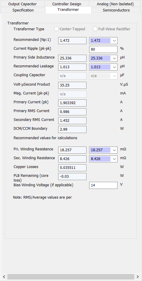
Transformer
WDS provides most necessary information such as “turns ratio”, “Volts-us” product etc. so that you or your magnetics design can design you’re the magnetics WDS recommends the transformer turns ratio Primary inductance and leakage. The user can of course change these values after which all calculation will be based on the user’s input. The user can also indicate if a bias winding is needed by filling in the “Bias Winding Voltage” box. Once all design parameters are completed in this tab the user can email this specification to his/her magnetics provider by pressing the “Generate and Email Transformer Design to” button on the “Summary” tab.
Isolated PSU Controller Design
Pole zero placement is identical to non-isolated version. In digital control, WDS assumes that the controller is on the secondary side with zero delay in transmitting the data to the primary side and therefore the design is identical to the non-isolated version. If there is a delay, this can be added in as a “Pure Time Delay” from the specifications tab.
For analog Isolated PSUs, WDS assumes that you will be using a traditional analog optocoupler. The pole zero placement stays identical but you must now add the parameters of your optocoupler. The circuit diagram of the type of isolated power supply that WDS designs is shown on the “Circuit” tab:
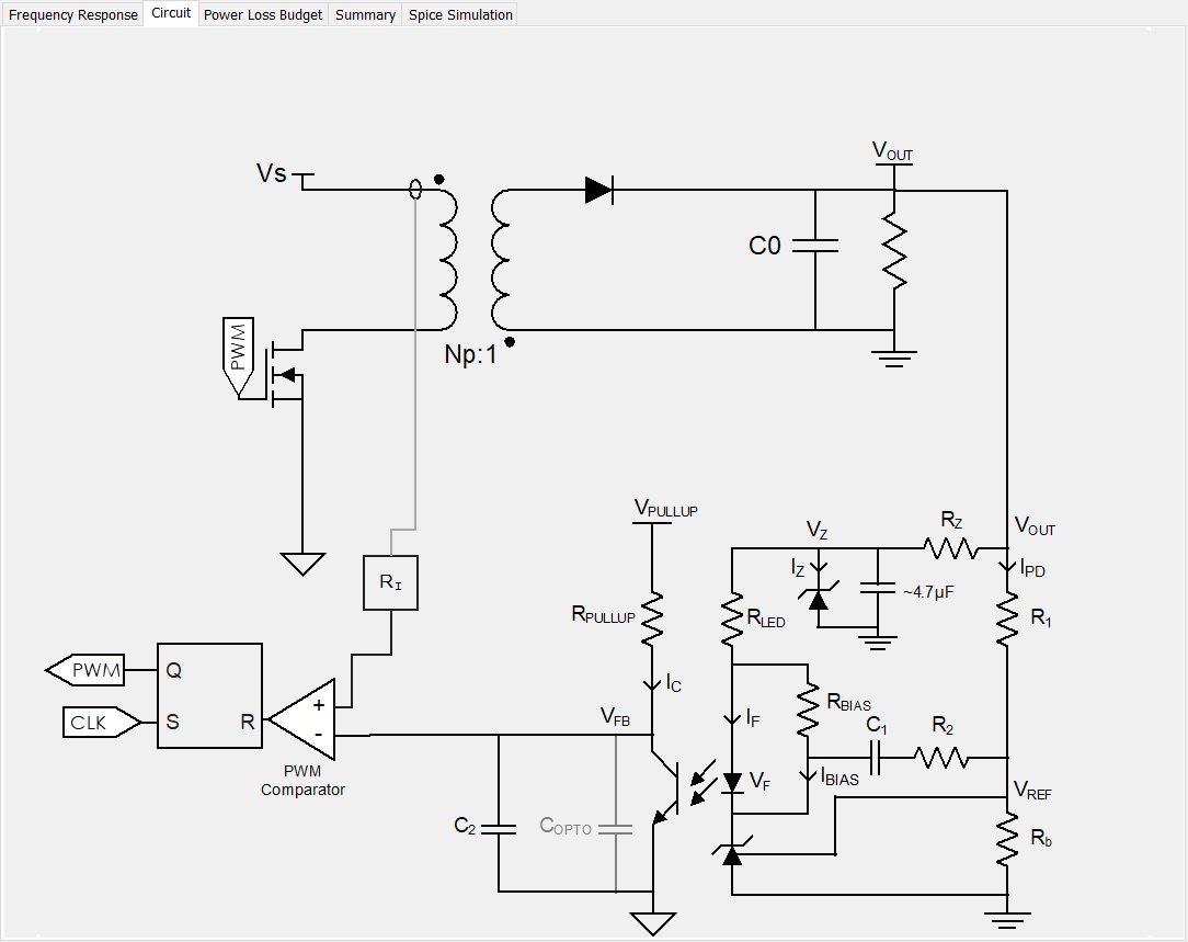
Using the above diagram the user must first input the data of their chosen optocoupler. This is done in the “Analog (Isolated)” tab.
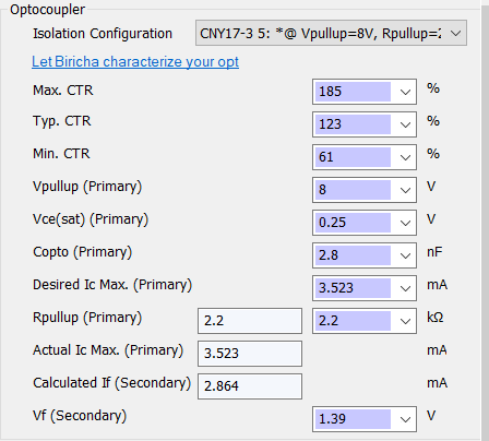
Maximum, Typical, Minimum CTR, forward drop across the diode (Vf) and Collector Emitter saturation voltage Vce(sat) are usually available from the manufacture’s datasheet. Copto represents the bandwidth of the opto and usually must be measured. Many good methods for measuring this parameter are freely available on-line.
Vpullup is the reference voltage from the user’s selected controller IC. Based on the above WDS calculates all other parameters which the user can of course change.
Finally, Zener reference voltage Vz must be operated in the breakdown region and therefore its value must be lower than the output voltage of the power supply. All other parameters are either available from the datasheet or are calculated by WDS.