
Voltage Mode Buck
In this tutorial, we will design a voltage mode Buck converter.
Preamble
Within WDS you will be presented with a selection of tabs, edit boxes and combo boxes. There is a general design methodology is that you should start with the "Specification" tab and work you way across to the "Analog (Non-Isolated)" tab updating the relevant parameters with your design choice along the way.
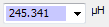
The default calculated values are always highlighted in purple as shown in the picture below.
In this tutorial, we will design a voltage mode Buck converter.
Preamble
Within WDS you will be presented with a selection of tabs, edit boxes and combo boxes. There is a general design methodology is that you should start with the "Specification" tab and work you way across to the "Analog (Non-Isolated)" tab updating the relevant parameters with your design choice along the way.
The default calculated values are always highlighted in purple as shown in the picture below.
You can edit this at any time by clicking into the box and overwriting them with your own value. The box will no longer be highlighted in purple indicating that your own value is being used.
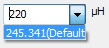
The value typed in by the user will always take precedence over the WDS calculated value. If at any time you wish to return to the default calculated value you can do so by clicking on the drop down arrow on the right hand side of the box and then selecting the option that says "(default)" next to it as shown in the screenshot below.
The value typed in by the user will always take precedence over the WDS calculated value. If at any time you wish to return to the default calculated value you can do so by clicking on the drop down arrow on the right hand side of the box and then selecting the option that says "(default)" next to it as shown in the screenshot below.
Specification
On the "Specification" tab, enter the following specification into the relevant fields under "Converter Specification":
On the "Specification" tab, enter the following specification into the relevant fields under "Converter Specification":
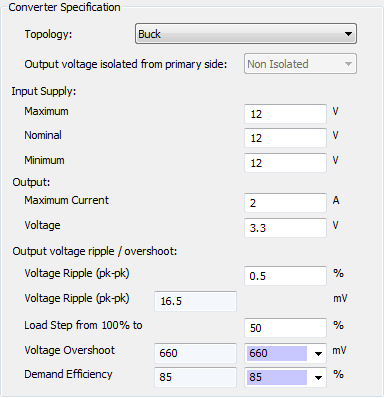
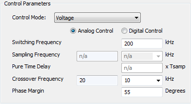
Again on the "Specification" tab, enter the following specification into the relevant fields under "Control Parameters":
As you update the values, WDS will automatically update the design and show the associated Bode plot in the Frequency Response tab.
Semiconductors
Now move onto the "Semiconductors" tab, enter the following specification into the relevant fields under "Primary Switch"; these are the actual parameters of the FETs that we are using on the board. Important: for now, please ignore the values in the left hand column; these are calculated values based on your specification and will get updated as you input various parameters in the future tabs.
Now move onto the "Semiconductors" tab, enter the following specification into the relevant fields under "Primary Switch"; these are the actual parameters of the FETs that we are using on the board. Important: for now, please ignore the values in the left hand column; these are calculated values based on your specification and will get updated as you input various parameters in the future tabs.
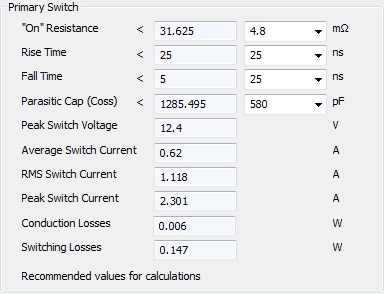
These are the values for the semiconductor switches that we are using on the Biricha Buck board used in our workshops.
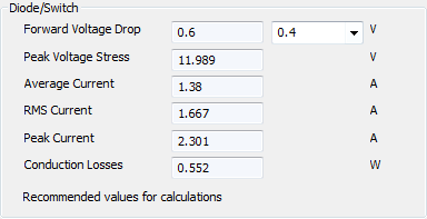
Again on the "Semiconductors" tab, enter the following specification into the relevant fields under "Diode/Switch":
Again on the "Semiconductors" tab, enter the following specification into the relevant fields under "Diode/Switch":
Output Filter
Now click on the "Output Filter" tab. On the "Output Filter" tab, enter the following specification into the relevant fields under "Output Filter Inductor ":
Now click on the "Output Filter" tab. On the "Output Filter" tab, enter the following specification into the relevant fields under "Output Filter Inductor ":
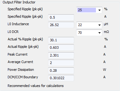
Again this is the parameters of the Wurth inductor that we are using on the Biricha Buck board.
Also on the "Output Filter" tab, enter the following specification into the relevant fields under "Output Filter Capacitor ":
Also on the "Output Filter" tab, enter the following specification into the relevant fields under "Output Filter Capacitor ":
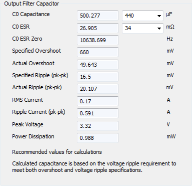
Note that we are using 2x220uF caps and we measured the ESR to be around 70mΩ for 1 capacitor. So the ESR of 2 in parallel will be around 34.5mΩ.
Controller Design
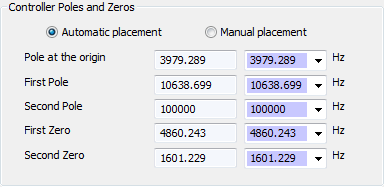
On the "Controller Design" tab, WDS has selected a Type III compensator. The automatic pole/zero placement algorithms have calculated the location of the poles and zeros such that the loop will achieve the crossover frequency and phase margin specification concurrently, i.e. WDS has designed a compensator that will give a crossover of 10kHz and a phase margin of 55 degrees. As shown below:
On the "Controller Design" tab, WDS has selected a Type III compensator. The automatic pole/zero placement algorithms have calculated the location of the poles and zeros such that the loop will achieve the crossover frequency and phase margin specification concurrently, i.e. WDS has designed a compensator that will give a crossover of 10kHz and a phase margin of 55 degrees. As shown below:
Note that in this tab WDS asks for the PWM ramp height which has been set to 1.8V
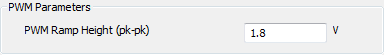
Note that this value is chip dependant. For the UC3823 chip that we are using the typical value from the datasheet is 1.8V.
If not already in context, click on the "Frequency Response" tab on the right hand side to view the simulated Bode plot. Under the “Bode Plot” section of this tab, make sure that only “Loop” is ticked. This will display the simulated loop response. See that the simulated crossover frequency and phase margin are displayed at the top of this tab.
Analog (Non-Isolated)
Click on the "Analog (Non-Isolated)" tab. The component values required for the Type III compensator have been automatically calculated.
In this example we will be using the UC3823 PWM controller from TI to implement the controller.
The voltage reference from this chip is 5.1V (from the datasheet). But, in this example, we divide this by 2 using a potential divider. Therefore in WDS please make sure that the “Error Amplifier Reference Voltage” is set to 2.55V.
Circuit Tab (right hand pane)
In WDS, click on the "Circuit" tab (right hand pane) and view the circuit diagram for the Type III compensator. Please study the circuit diagram and identify the location of the Type III compensator components.
Frequency Response
Click on the "Frequency Response" tab again to view the Bode plot. Then observe how the Bode plot changes as you type in the Nearest Preferred Values (NPVs) used in the actual circuit in to the relevant boxes in the "Controller Component Values" section of the "Analog (Non-Isolated)". The component values are shown below:
Click on the "Frequency Response" tab again to view the Bode plot. Then observe how the Bode plot changes as you type in the Nearest Preferred Values (NPVs) used in the actual circuit in to the relevant boxes in the "Controller Component Values" section of the "Analog (Non-Isolated)". The component values are shown below:
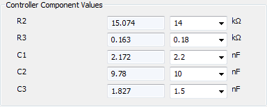
WDS will always use the user defined values instead of calculated values. So now that you have changed the component values to their NPVs, your crossover and phase margin will also have changed. The simulated crossover frequency and phase margin have changed because you have now entered the values of the components used on the actual PCB, which are slightly different to those calculated by WDS. Thus your compensator poles and zeros are slightly different from the ones calculated by WDS.
Power Loss Budget Tab (right hand pane)
This tab toughly estimates the total power loss in various components of the power supply.
Total power loss budget (PLB) is estimated based on the user’s efficiency requirements and this is displayed at the bottom light hand side of the WDS window. A warning is displayed of the losses exceed the total PLB.
Summary Tab (right hand pane)
This is the final summary of your design. It includes all the parameters calculated by WDS including all the voltage and current stresses on the devices in addition to all the frequency repose Bode plots.
When your design is complete, you can save this as an rft file by pressing the “Save Summary As” button or insert on your own reports by simply copying and pasting.
Finally pressing “Generate and Email Transformer Design to” allows you to generate an email with all the parameters relevant to the transformer which you can send to your magnetics supplier of choice.
Spice Simulation Tab (right hand pane)
This is an extremely power full feature full explanation of the available simulations is given when you click on this tab.