
Digital Voltage Mode Buck
In this tutorial, we will design a digital controller using WDS.
Preamble
Within WDS you will be presented with a selection of tabs, edit boxes and combo boxes. There is a general design methodology is that you should start with the "Specification" tab and work you way across to the "Analog (Non-Isolated)" tab updating the relevant parameters with your design choice along the way.
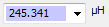
The default calculated values are always highlighted in purple as shown in the picture below.
In this tutorial, we will design a digital controller using WDS.
Preamble
Within WDS you will be presented with a selection of tabs, edit boxes and combo boxes. There is a general design methodology is that you should start with the "Specification" tab and work you way across to the "Analog (Non-Isolated)" tab updating the relevant parameters with your design choice along the way.
The default calculated values are always highlighted in purple as shown in the picture below.
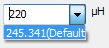
You can edit this at any time by clicking into the box and overwriting them with your own value. The box will no longer be highlighted in purple indicating that your own value is being used.
The value typed in by the user will always take precedence over the WDS calculated value. If at any time you wish to return to the default calculated value you can do so by clicking on the drop down arrow on the right hand side of the box and then selecting the option that says "(default)" next to it as shown in the screenshot below.
The value typed in by the user will always take precedence over the WDS calculated value. If at any time you wish to return to the default calculated value you can do so by clicking on the drop down arrow on the right hand side of the box and then selecting the option that says "(default)" next to it as shown in the screenshot below.
Specification
On the "Specification" tab, enter the following specification into the relevant fields under "Converter Specification":
On the "Specification" tab, enter the following specification into the relevant fields under "Converter Specification":
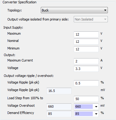
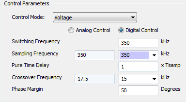
Again on the "Specification" tab, enter the following specification into the relevant fields under "Control Parameters":
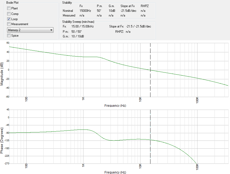
As you update the values, WDS will automatically update the design and show the associated Bode plot in the Frequency Response tab.
Semiconductors
Now move onto the "Semiconductors" tab, enter the following specification into the relevant fields under "Primary Switch"; these are the actual parameters of the FETs that we are using on the board. Important: for now, please ignore the values in the left hand column; these are calculated values based on your specification and will get updated as you input various parameters in the future tabs.
Now move onto the "Semiconductors" tab, enter the following specification into the relevant fields under "Primary Switch"; these are the actual parameters of the FETs that we are using on the board. Important: for now, please ignore the values in the left hand column; these are calculated values based on your specification and will get updated as you input various parameters in the future tabs.
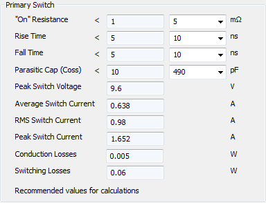
These are the values for the semiconductor switches that we are using on the Biricha Buck board used in our workshops.
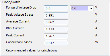
Again on the "Semiconductors" tab, enter the following specification into the relevant fields under "Diode/Switch":
Again on the "Semiconductors" tab, enter the following specification into the relevant fields under "Diode/Switch":
Output Filter
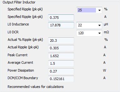
Now click on the "Output Filter" tab. On the "Output Filter" tab, enter the following specification into the relevant fields under "Output Filter Inductor ":
Now click on the "Output Filter" tab. On the "Output Filter" tab, enter the following specification into the relevant fields under "Output Filter Inductor ":
Again this is the parameters of the Wurth inductor that we are using on the Biricha Buck board.
Also on the "Output Filter" tab, enter the following specification into the relevant fields under "Output Filter Capacitor ":
Also on the "Output Filter" tab, enter the following specification into the relevant fields under "Output Filter Capacitor ":
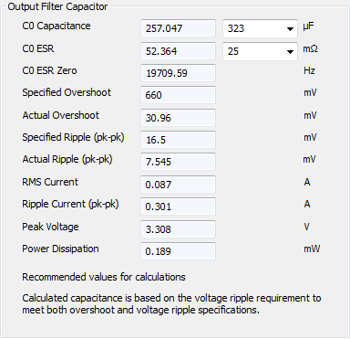
Note that we are using 2x220uF caps and we measured the ESR to be around 70mΩ for 1 capacitor. So the ESR of 2 in parallel will be around 34.5mΩ.
Controller Design
On the "Controller Design" tab, WDS has selected a Type III compensator. The automatic pole/zero placement algorithms have calculated the location of the poles and zeros such that the loop will achieve the crossover frequency and phase margin specification concurrently, i.e. WDS has designed a compensator that will give a crossover of 15kHz and a phase margin of 50 degrees (after phase erosion). As shown below:
On the "Controller Design" tab, WDS has selected a Type III compensator. The automatic pole/zero placement algorithms have calculated the location of the poles and zeros such that the loop will achieve the crossover frequency and phase margin specification concurrently, i.e. WDS has designed a compensator that will give a crossover of 15kHz and a phase margin of 50 degrees (after phase erosion). As shown below:
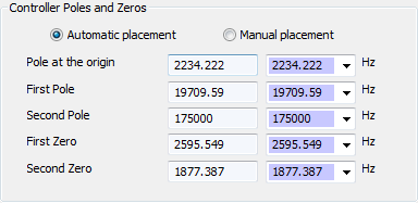
If not already in context, click on the "Frequency Response" tab on the right hand side to view the simulated Bode plot. Under the "Bode Plot" section of this tab, make sure that only "Loop" is ticked. This will display the simulated loop response. See that the simulated crossover frequency and phase margin are displayed at the top of this tab.
Digital (Non-Isolated)
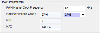
Click on the "Digital (Non-Isolated)" tab, enter the following into the relevant fields under "PWM Parameters"
Click on the "Digital (Non-Isolated)" tab, enter the following into the relevant fields under "PWM Parameters"
Again on the "Digital (Non-Isolated)" tab, enter the following into the relevant fields under "Sampling Divider and ADC":
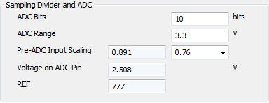
WDS will now be able to calculate the correct scaling factors for the digital controller.
Coeffs
WDS can provide the coefficients in various formats. Generic Fixed and Floating point, TI IQ format, Microchip MCU16, ST MCU32 and Infineon XMC. For the purpose of this example we only present Microchip’s 16 but fixed point format however the general principle stays the same for all other formats.
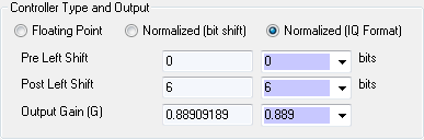
Click on the "Coeffs (Fixed Point / Microchip)" tab (on the right hand pane of WDS), and select "Normalized (IQ Format)" from the "Controller Type and Output" group as per the image below.
WDS can provide the coefficients in various formats. Generic Fixed and Floating point, TI IQ format, Microchip MCU16, ST MCU32 and Infineon XMC. For the purpose of this example we only present Microchip’s 16 but fixed point format however the general principle stays the same for all other formats.
Click on the "Coeffs (Fixed Point / Microchip)" tab (on the right hand pane of WDS), and select "Normalized (IQ Format)" from the "Controller Type and Output" group as per the image below.
WDS will then calculate the correct controller coefficients.
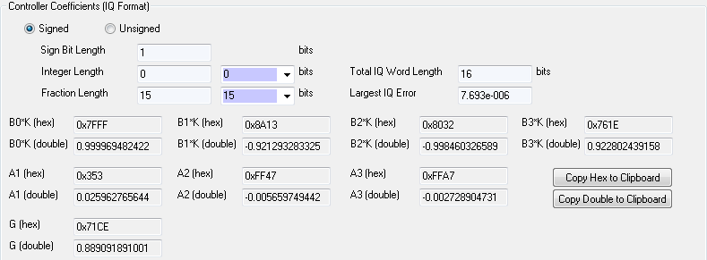
The user simply clicks "Copy Hex to Clipboard" and then pastes the controller coefficients directly into their code.
Implementation and Results
The design is now complete!
The completed WDS file used in this tutorial can be downloaded from the resources section of our main website along with the MPLAB example project.
Implementation and Results
The design is now complete!
The completed WDS file used in this tutorial can be downloaded from the resources section of our main website along with the MPLAB example project.